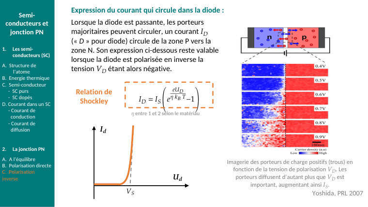
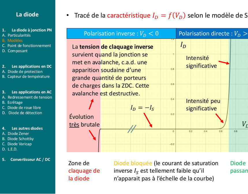
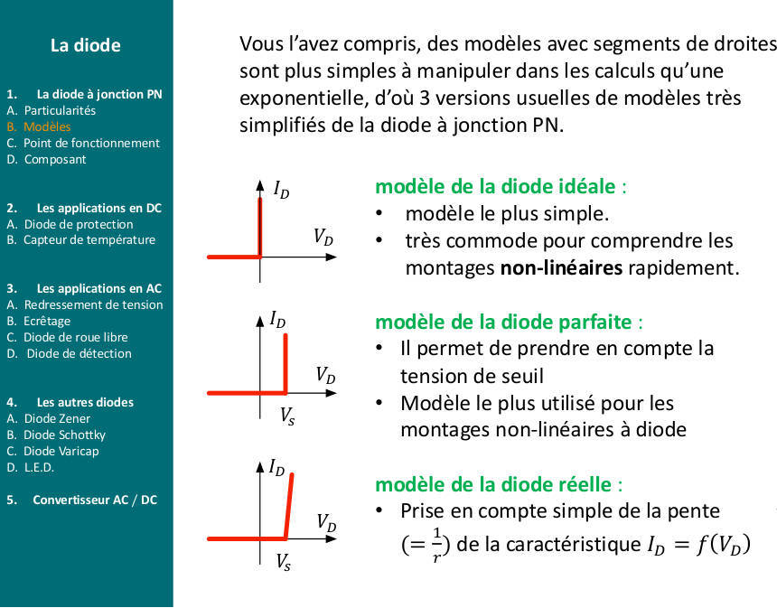
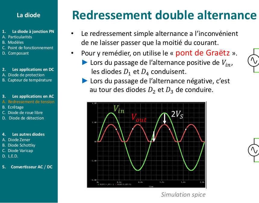
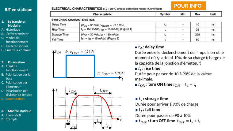
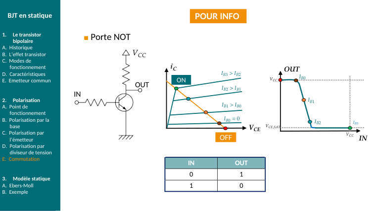
En électronique, 80 % de la réussite est dans les 30 premières secondes : reconnaître le type de problème et poser la bonne hypothèse.
E1Ch. 0 · Thévenin
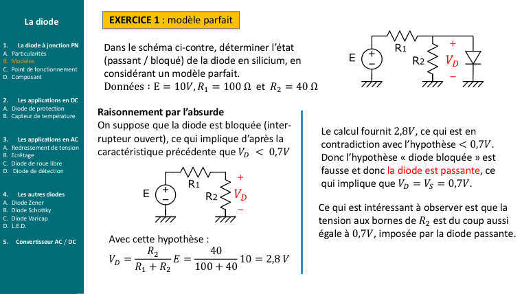
Pont diviseur chargé : \(V_{\mathrm{CC}}=12\,\mathrm{V},\,\allowbreak R_{1}=4\,\mathrm{k\Omega },\,\allowbreak R_{2}=8\,\mathrm{k\Omega }\), charge \(R_{L}=8\,\mathrm{k\Omega }\) aux bornes de \(R_{2}\)
Ce qu'on chercheLa tension \(V_{L}\) aux bornes de la charge. Piège : le diviseur de tension « nu » donne \(8\,\mathrm{V}\), mais la charge tire du courant et fait chuter la tension. Thévenin règle ça proprement.
Tension à vide (on enlève \(R_{L}\))
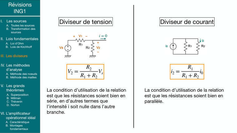
\(\displaystyle V_{\mathrm{Th}}=V_{\mathrm{CC}}\,\cdot \,\frac{R_{2}}{R_{1}+R_{2}}=12\,\cdot \,\frac{8}{12}=8\,\mathrm{V}\)
Résistance vue de \(A-B\), source neutralisée (\(V_{\mathrm{CC}}\to\) fil)
\(R_{1}\) et \(R_{2}\) se retrouvent en parallèle :
\(\displaystyle R_{\mathrm{Th}}=R_{1}//R_{2}=\frac{4\cdot 8}{4+8}=\frac{32}{12}\approx 2{,}67\,\mathrm{k\Omega }\)
Remettre la charge sur le générateur équivalent
\(\displaystyle V_{L}=V_{\mathrm{Th}}\,\cdot \,\frac{R_{L}}{R_{\mathrm{Th}}+R_{L}}=8\,\cdot \,\frac{8}{2{,}67+8}=8\,\cdot \,0{,}75=6\,\mathrm{V}\)
Contrôle sans Thévenin
\(R_{2}//R_{L}=4\,\mathrm{k\Omega }\), diviseur : \(12\,\cdot \,\frac{4}{4+4}=6\,\mathrm{V}\) ✓. Norton au passage : \(I_{N}=\frac{V_{\mathrm{Th}}}{R_{\mathrm{Th}}}=3\,\mathrm{mA}\).
Réponse\(V_{\mathrm{Th}}=8\,\mathrm{V},\,\allowbreak R_{\mathrm{Th}}=2{,}67\,\mathrm{k\Omega },\,\allowbreak V_{L}=6\,\mathrm{V}\) (et non \(8\,\mathrm{V}!\)).
Pourquoi ThéveninDès que la charge varie, on ne refait pas tout le circuit : on garde \((V_{\mathrm{Th}},\,\allowbreak R_{\mathrm{Th}})\) et on ne change que \(R_{L}\). Règle pratique : un pont diviseur se comporte en source de tension si \(R_{L}\gg R_{\mathrm{Th}}\) (ici \(8\,\mathrm{k}\) n'est pas \(\gg 2{,}67\,\mathrm{k}\), d'où la chute de 25 %).
E2Ch. 0 · AOP et décibels
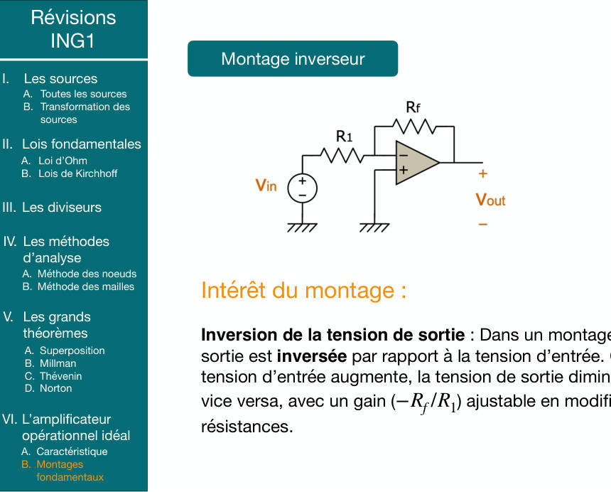
Non-inverseur \(R_{1}=1\,\mathrm{k\Omega },\,\allowbreak R_{f}=9\,\mathrm{k\Omega }\) ; puis inverseur \(R_{1}=2\,\mathrm{k\Omega },\,\allowbreak R_{f}=10\,\mathrm{k\Omega }\) ; alimentation \(\pm 15\,\mathrm{V}\)
Ce qu'on chercheLe gain de chaque montage, en linéaire et en dB, et la plage de \(V_{\mathrm{in}}\) pour laquelle l'AOP reste en régime linéaire.
Vérifier le régime
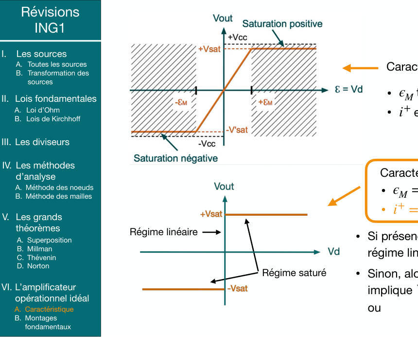
\(R_{f}\) relie la sortie à l'entrée − : contre-réaction négative ⟹ régime linéaire \(\Longrightarrow V_{+}=V_{-}\) et \(i_{\pm }=0\).
Non-inverseur : loi des nœuds à l'entrée −
\(V_{-}=V_{\mathrm{in}}\) est le point milieu du diviseur \(\frac{R_{1}}{R_{f}}\) alimenté par \(V_{\mathrm{out}}\) :
\(\displaystyle V_{\mathrm{in}}=V_{\mathrm{out}}\,\cdot \,\frac{R_{1}}{R_{1}+R_{f}}\Longrightarrow A=\frac{V_{\mathrm{out}}}{V_{\mathrm{in}}}=1+\frac{R_{f}}{R_{1}}=1+9=10\Longrightarrow 20\cdot \log (10)=20\,\mathrm{d}B\)
Inverseur : \(V_{-}=V_{+}=0\) (masse virtuelle)
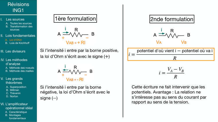
\(\displaystyle i=\frac{V_{\mathrm{in}}}{R_{1}}\text{ traverse }\,R_{f}\,(i_{-}=0)\colon V_{\mathrm{out}}=0-R_{f}\,\cdot \,i=-\left(\frac{R_{f}}{R_{1}}\right)\cdot V_{\mathrm{in}}=-5\cdot V_{\mathrm{in}}\)
\(\displaystyle |A|=5\Longrightarrow 20\cdot \log (5)\approx 14\,\mathrm{d}B\,(\text{le signe }-\text{ est un déphasage de }\,180\text{°},\,\allowbreak \text{ pas un gain négatif en }\,\mathrm{d}B)\)
Plage linéaire
La sortie ne peut pas dépasser \(\pm V_{\mathrm{sat}}\approx \pm 15\,\mathrm{V}\) (souvent \(\pm 13-14\,\mathrm{V}\) en réel). Non-inverseur : \(|V_{\mathrm{in}}|\lt \frac{15}{10}=1{,}5\,\mathrm{V}\). Inverseur : \(|V_{\mathrm{in}}|\lt 3\,\mathrm{V}\). Au-delà, \(V_{\mathrm{out}}=\pm V_{\mathrm{sat}}\) (écrêtage).
Réponse\(A=+10\,(20\,\mathrm{d}B)\), linéaire pour \(|V_{\mathrm{in}}|\lt 1{,}5\,\mathrm{V};\,\allowbreak A=-5\,(14\,\mathrm{d}B)\), linéaire pour \(|V_{\mathrm{in}}|\lt 3\,\mathrm{V}\).
Table dB à connaître\(\times 1=0\,\mathrm{d}B,\,\allowbreak \times \sqrt{2}=3\,\mathrm{d}B,\,\allowbreak \times 2=6\,\mathrm{d}B,\,\allowbreak \times 10=20\,\mathrm{d}B,\,\allowbreak \times 100=40\,\mathrm{d}B\). Pour un gain en puissance c'est \(10\cdot \log\) (car \(P\,\propto \,V^{2}\)). Un gain \(0{,}5=-6\,\mathrm{d}B\) (atténuation).
E3Ch. 1 · Conduction
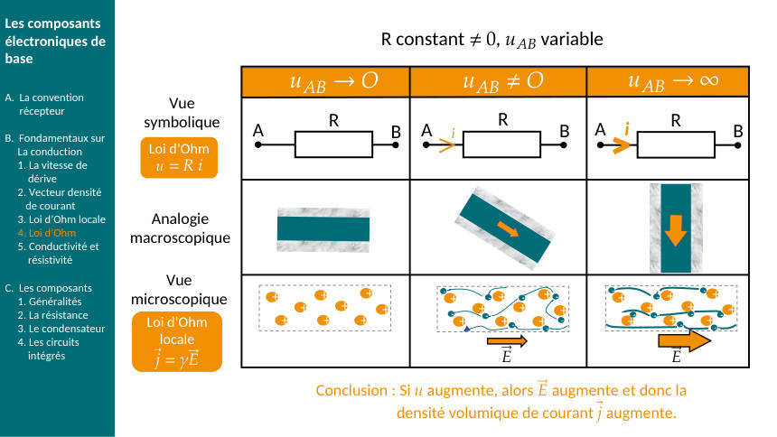
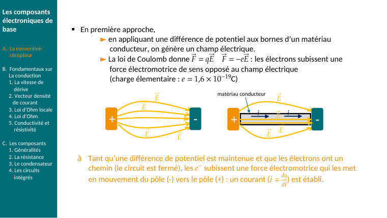
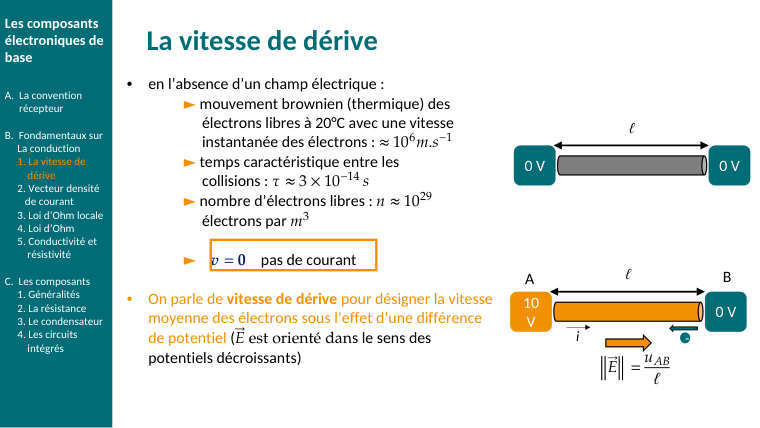
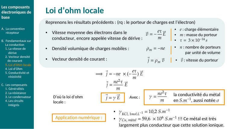
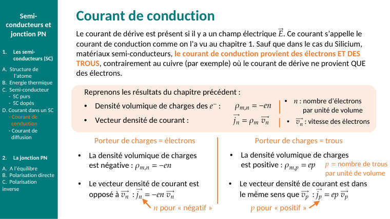
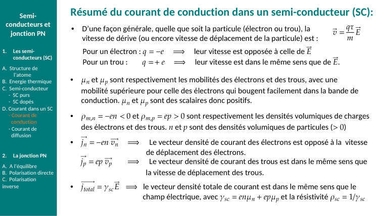
Fil de cuivre \(\ell =10\,\mathrm{m}\), diamètre \(1\,\mathrm{mm},\,\allowbreak \rho =1{,}7\cdot 10^{-8}\,\mathrm{\Omega }\cdot m\), parcouru par \(i=2\,\mathrm{A}\). Calculer \(R,\,\allowbreak u,\,\allowbreak j,\,\allowbreak E\) et la vitesse de dérive \((n=8{,}5\cdot 10^{28}\,\mathrm{m}^{-3})\).
Ce qu'on chercheUne chaîne de formules, chacune à une ligne. Le seul danger : les unités (mm \(\to m\), section \(=\pi r^{2}\) avec le rayon).
Section et résistance
\(\displaystyle S=\pi \,r^{2}=\pi \,(0{,}5\cdot 10^{-3})^{2}=7{,}85\cdot 10^{-7}\,\mathrm{m}^{2}\)
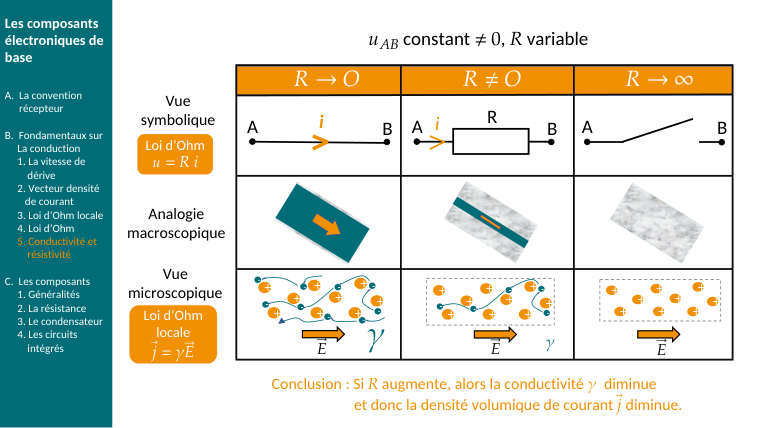
\(\displaystyle R=\rho \,\ell \,/\,S=1{,}7\cdot 10^{-8}\,\cdot \,10\,/\,7{,}85\cdot 10^{-7}\approx 0{,}22\,\mathrm{\Omega }\)
Tension, champ, densité de courant
\(\displaystyle u=R\,i=0{,}22\,\cdot \,2\approx 0{,}43\,\mathrm{V}\,E=\frac{u}{\ell }=0{,}043\,\mathrm{V}/\,\mathrm{m}\)
\(\displaystyle j=\frac{i}{S}=2\,/\,7{,}85\cdot 10^{-7}\approx 2{,}5\cdot 10^{6}\,\mathrm{A}/\,\mathrm{m}^{2}\,\left(\text{vérif }\colon j=\gamma E=\left(\frac{1}{\rho }\right)\cdot E=5{,}9\cdot 10^{7}\,\cdot \,0{,}043\approx 2{,}5\cdot 10^{6}\text{ ✓}\right)\)
Vitesse de dérive
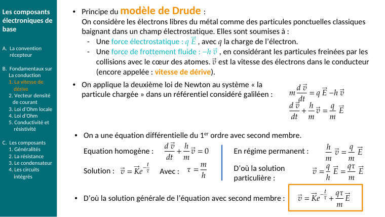
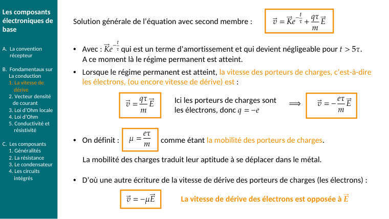
\(\displaystyle j=n\,e\,v\Longrightarrow v=\frac{j}{(n\,e)}=2{,}5\cdot 10^{6}\,/\,(8{,}5\cdot 10^{28}\,\cdot \,1{,}6\cdot 10^{-19})=2{,}5\cdot 10^{6}\,/\,1{,}36\cdot 10^{10}\approx 1{,}9\cdot 10^{-4}\,\mathrm{m}/\,\mathrm{s}\approx 0{,}2\,\mathrm{mm}/\,\mathrm{s}\)
Mobilité (bonus)
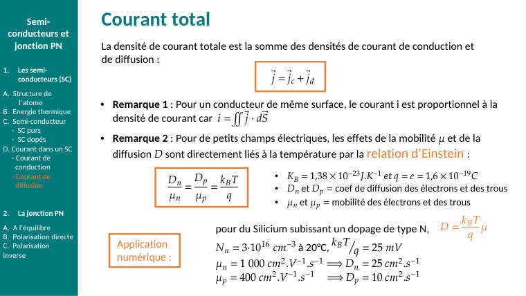
\(v=\mu E\Longrightarrow \mu =\frac{v}{E}=1{,}9\cdot \frac{10^{-4}}{0{,}043}\approx 4{,}3\cdot 10^{-3}\,\mathrm{m}^{2}/V\cdot s\). Ordre de grandeur correct pour le cuivre.
Réponse\(R\approx 0{,}22\,\mathrm{\Omega };\,\allowbreak u\approx 0{,}43\,\mathrm{V};\,\allowbreak j\approx 2{,}5\cdot 10^{6}\,\mathrm{A}/\,\mathrm{m}^{2};\,\allowbreak v\approx 0{,}2\,\mathrm{mm}/\,\mathrm{s}\).
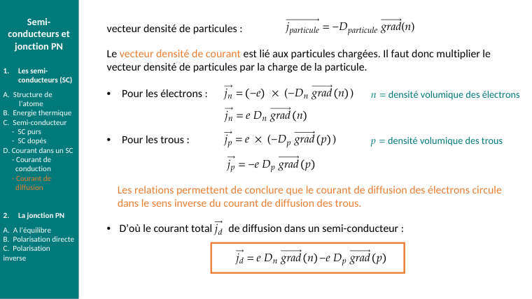
L'ordre de grandeur à retenirLa vitesse de dérive des électrons est de l'ordre du \(\frac{mm}{s}\) alors que le signal se propage quasi à la vitesse de la lumière : ce qui se propage, c'est le champ \(E\), pas les électrons.
E4Ch. 2 · Dopage
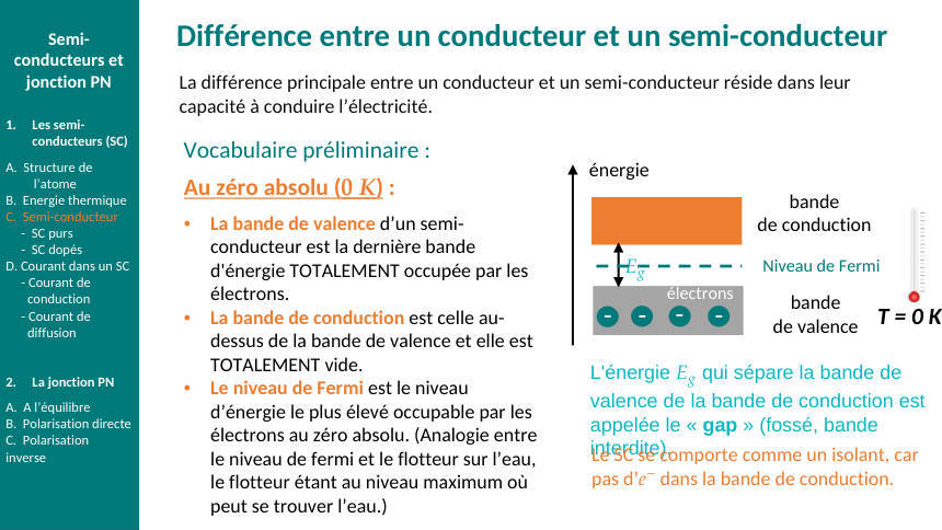
Silicium dopé au phosphore \(N_{D}=10^{16}\,\mathrm{cm}^{-3}\) à \(300\,\mathrm{K}\,(n_{i}=1{,}5\cdot 10^{10}\,\mathrm{cm}^{-3},\,\allowbreak \mu _{n}=1350,\,\allowbreak \mu _{p}=480\,\mathrm{cm}^{2}/V\cdot s)\)
Ce qu'on chercheLe type, les densités \(n\) et \(p\), la conductivité et la résistivité. Puis comparer au silicium intrinsèque.
Identifier
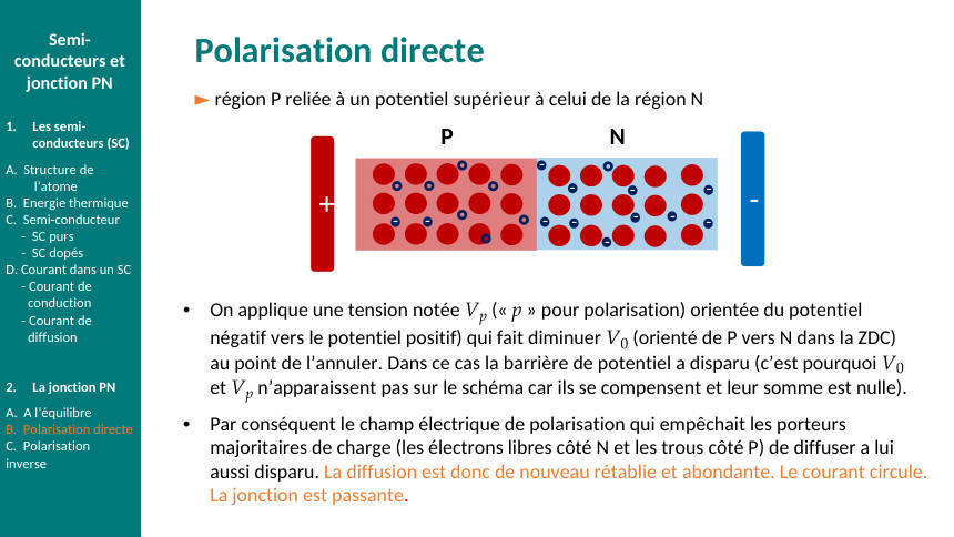
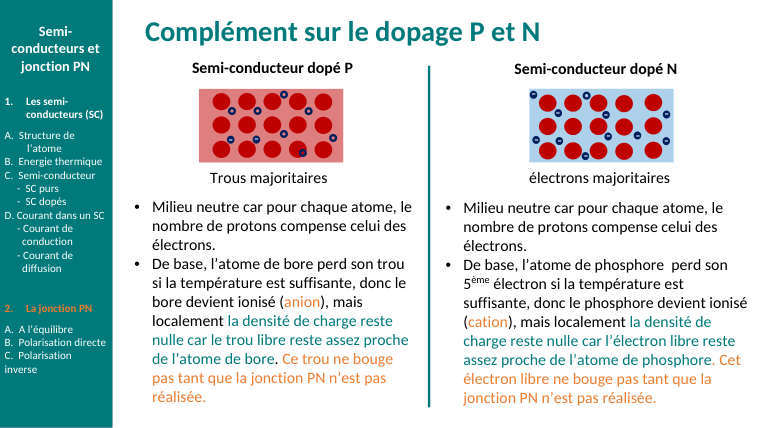
Phosphore : groupe \(V,\,\allowbreak 5\) électrons de valence ⟹ donneur ⟹ type \(\mathbf{N}\), électrons majoritaires.
Densités \((N_{D}\gg n_{i})\)
\(\displaystyle n\approx N_{D}=10^{16}\,\mathrm{cm}^{-3}\)
\(\displaystyle p=\frac{n_{i}^{2}}{N_{D}}=(1{,}5\cdot 10^{10})^{2}\,/\,10^{16}=2{,}25\cdot 10^{20}\,/\,10^{16}=2{,}25\cdot 10^{4}\,\mathrm{cm}^{-3}\)
Rapport \(\frac{n}{p}\approx 4\cdot 10^{11}\) : les trous sont totalement négligeables.
Conductivité (en unités cm : \(e\) en \(C,\,\allowbreak n\) en \(cm^{-3},\,\allowbreak \mu\) en \(\frac{cm^{2}}{V}\cdot s\Longrightarrow \gamma\) en \(\frac{S}{cm}\))
\(\displaystyle \gamma =e\,(n\,\mu _{n}+p\,\mu _{p})\approx 1{,}6\cdot 10^{-19}\,\cdot \,10^{16}\,\cdot \,1350\approx 2{,}2\,\mathrm{S}/cm\Longrightarrow \rho =\frac{1}{\gamma }\approx 0{,}46\,\mathrm{\Omega }\cdot \text{cm}\)
Comparaison avec l'intrinsèque
\(\displaystyle \gamma _{i}=e\,n_{i}\,(\mu _{n}+\mu _{p})=1{,}6\cdot 10^{-19}\,\cdot \,1{,}5\cdot 10^{10}\,\cdot \,1830\approx 4{,}4\cdot 10^{-6}\,\mathrm{S}/cm\)
Le dopage à 1 atome pour ~5 millions (\(10^{16}\,/\,5\cdot 10^{22}\) atomes de Si) multiplie la conductivité par ~500 000. C'est tout le principe du semi-conducteur.
RéponseType \(N;\,\allowbreak n=10^{16}\,\mathrm{cm}^{-3},\,\allowbreak p=2{,}25\cdot 10^{4}\,\mathrm{cm}^{-3};\,\allowbreak \gamma \approx 2{,}2\,\mathrm{S}/cm,\,\allowbreak \rho \approx 0{,}46\,\mathrm{\Omega }\cdot\)cm.
Piège d'unitésSi l'énoncé mélange \(cm^{-3}\) et \(\frac{m^{2}}{V}\cdot s\), tout convertir : \(10^{16}\,\mathrm{cm}^{-3}=10^{22}\,\mathrm{m}^{-3};\,\allowbreak 1350\,\mathrm{cm}^{2}/V\cdot s=0{,}135\,\mathrm{m}^{2}/V\cdot s\). Alors \(\gamma =1{,}6\cdot 10^{-19}\,\cdot \,10^{22}\,\cdot \,0{,}135=216\,\mathrm{S}/\,\mathrm{m}=2{,}16\,\mathrm{S}/cm\) ✓ \((1\,\mathrm{S}/cm=100\,\mathrm{S}/\,\mathrm{m})\).
E5Ch. 2 · Jonction PN
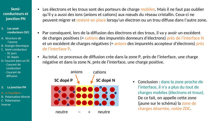
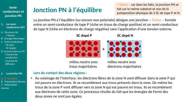
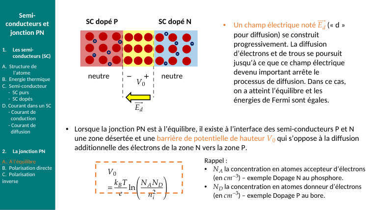
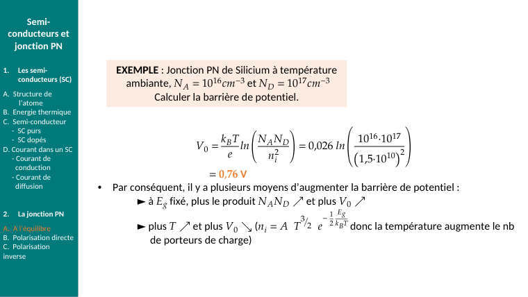
Barrière de potentiel d'une jonction Si avec \(N_{A}=10^{17}\,\mathrm{cm}^{-3},\,\allowbreak N_{D}=10^{16}\,\mathrm{cm}^{-3}\) à \(300\,\mathrm{K}\)
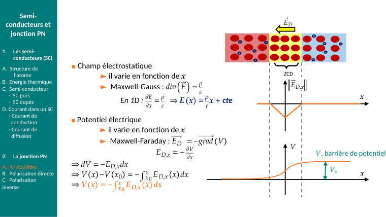
Ce qu'on cherche\(V_{0}\), puis l'effet d'une hausse de température et d'un dopage plus fort. Formule : \(V_{0}=\left(\frac{k_{B}T}{e}\right)\cdot \ln \left(\frac{N_{A}N_{D}}{n_{i}^{2}}\right)\).
Tension thermique
\(\displaystyle k_{B}\,T\,/\,e=1{,}38\cdot 10^{-23}\,\cdot \,300\,/\,1{,}6\cdot 10^{-19}\approx 0{,}026\,\mathrm{V}=26\,\mathrm{mV}\)
À retenir par cœur, c'est aussi le \(V_{T}\) de \(r_{E}=26\,\mathrm{mV}/I_{E}\).
Argument du logarithme
\(\displaystyle N_{A}\,N_{D}\,/\,n_{i}^{2}=10^{17}\,\cdot \,10^{16}\,/\,(1{,}5\cdot 10^{10})^{2}=10^{33}\,/\,2{,}25\cdot 10^{20}\approx 4{,}4\cdot 10^{12}\)
\(\displaystyle \ln (4{,}4\cdot 10^{12})=\ln \,4{,}4+12\cdot \ln \,10\approx 1{,}48+27{,}6\approx 29{,}1\)
Barrière
\(\displaystyle V_{0}=0{,}026\,\cdot \,29{,}1\approx 0{,}76\,\mathrm{V}\)
Cohérent avec la valeur « typique » du cours et proche du seuil \(0{,}7\,\mathrm{V}\) de la diode.
Variations
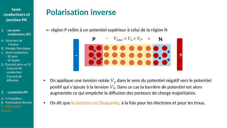
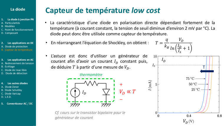
Dopage \(\times 10\) sur \(N_{D}\Longrightarrow \ln\) augmente de \(\ln \,10=2{,}3\Longrightarrow V_{0}+60\,\mathrm{mV}\). \(T\) qui monte \(\Longrightarrow n_{i}\) explose \(\left(e^{\frac{-E_{g}}{2}\,\mathrm{kT}}\right)\Longrightarrow\) l'argument \(\mathrm{d}u\,\ln\) chute plus vite que \(\frac{kT}{e}\) ne monte ⟹ \(V_{0}\) diminue (\(\approx -2\,\mathrm{mV}/^{\circ}\mathrm{C}\), c'est le capteur de température à diode).
Réponse\(V_{0}\approx 0{,}76\,\mathrm{V}\).
Calculer un \(\ln\) sans calculatrice\(\ln (a\cdot 10^{k})=\ln \,a+2{,}3\cdot k\). Avec \(\ln \,2\approx 0{,}69,\,\allowbreak \ln \,3\approx 1{,}1,\,\allowbreak \ln \,5\approx 1{,}6\), on encadre n'importe quel logarithme à 5 % près.
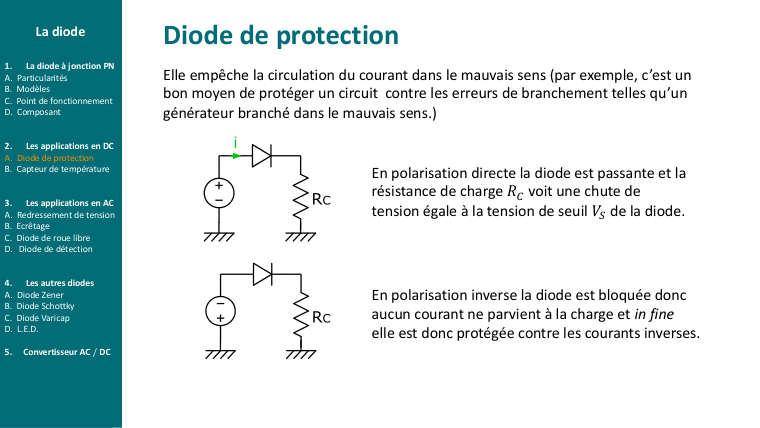
E6Ch. 3 · État d'une diode
Source \(E\) en série avec \(R=1\,\mathrm{k\Omega }\) et une diode Si. Cas \((a)\,E=5\,\mathrm{V}\) dans le sens passant ; \((b)\,E=0{,}5\,\mathrm{V};\,\allowbreak (c)\,E=5\,\mathrm{V}\), diode retournée. Modèle parfait, puis réel avec \(r=10\,\mathrm{\Omega }\).
Ce qu'on chercheL'état de la diode et le point de fonctionnement \((V_{D},\,\allowbreak I_{D})\) dans chaque cas, par la méthode de l'hypothèse.
(a) Hypothèse « bloquée »
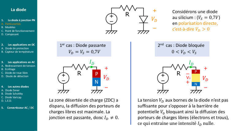
\(I_{D}=0\Longrightarrow\) pas de chute dans \(R\Longrightarrow V_{D}=E=5\,\mathrm{V}\). Or une diode bloquée doit avoir \(V_{D}\lt 0{,}7\,\mathrm{V}\) : contradiction ⟹ elle est passante.
(a) Hypothèse « passante », modèle parfait \(V_{D}=0{,}7\,\mathrm{V}\)
\(\displaystyle \text{Maille }\colon E-R\,I_{D}-V_{S}=0\Longrightarrow I_{D}=\frac{E-V_{S}}{R}=\frac{5-0{,}7}{1000}=4{,}3\,\mathrm{mA}\gt 0\text{ ✓ cohérent}\)
(a) Modèle réel
\(\displaystyle I_{D}=\frac{E-V_{S}}{R+r}=\frac{4{,}3}{1010}\approx 4{,}26\,\mathrm{mA};\,\allowbreak V_{D}=V_{S}+r\,I_{D}=0{,}7+0{,}043\approx 0{,}74\,\mathrm{V}\)
Différence de 1 % : le modèle parfait suffit dès que \(R\gg r\).
\((b)\,E=0{,}5\,\mathrm{V}\)
Hypothèse bloquée : \(V_{D}=0{,}5\,\mathrm{V}\lt 0{,}7\,\mathrm{V}\) ✓ cohérent ⟹ bloquée, \(I_{D}=0,\,\allowbreak V_{R}=0\). (Hypothèse passante donnerait \(I_{D}=\frac{0{,}5-0{,}7}{R}\lt 0\) : absurde.)
\((c)\) Diode en inverse
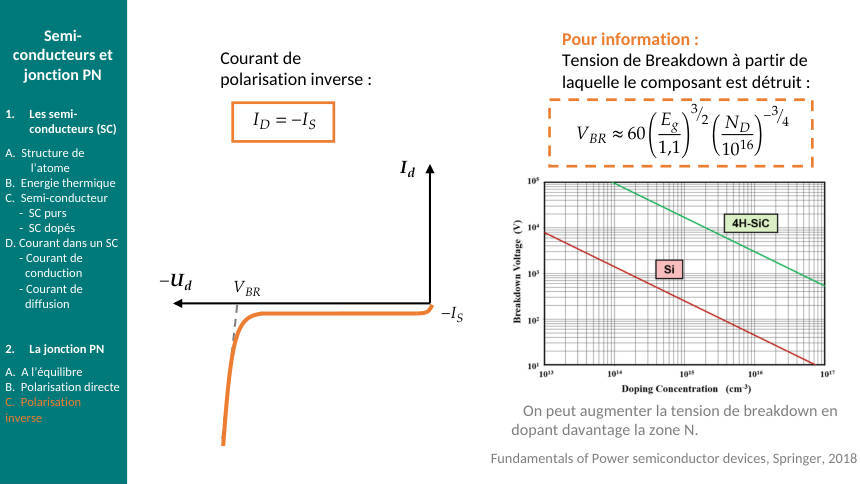
Hypothèse bloquée : \(V_{D}=-5\,\mathrm{V}\lt 0{,}7\) ✓ ⟹ bloquée. Vérifier que \(|-5\,\mathrm{V}|\lt V_{\mathrm{BR}}\) (ex. \(100\,\mathrm{V}\) pour une 1N4148) : pas de claquage. Toute la tension \(E\) est aux bornes de la diode.
Réponse(a) passante, \(I_{D}=4{,}3\,\mathrm{mA},\,\allowbreak V_{D}=0{,}7\,\mathrm{V}\) (\(0{,}74\,\mathrm{V}\) en réel) ; \((b)\) bloquée ; \((c)\) bloquée, \(V_{D}=-5\,\mathrm{V}\).
Avec plusieurs diodesMême méthode : on suppose un état pour chaque diode (2 diodes = 4 combinaisons), on calcule, on vérifie toutes les conditions. Commencer par l'hypothèse la plus plausible (celle où la source « pousse » dans le sens passant).
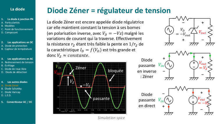
E7Ch. 3 · Régulateur Zener
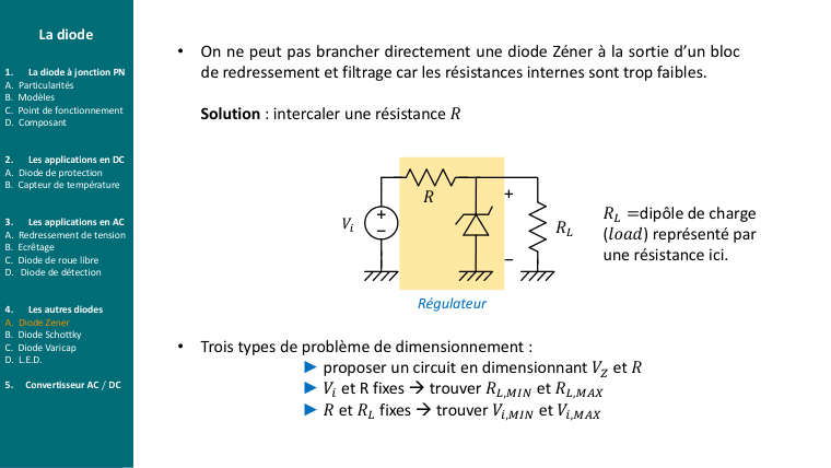
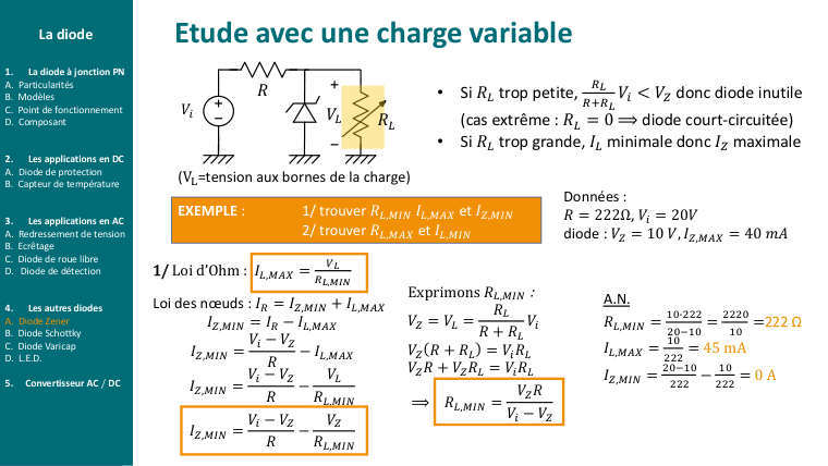
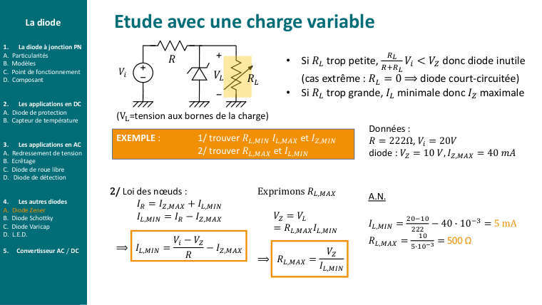
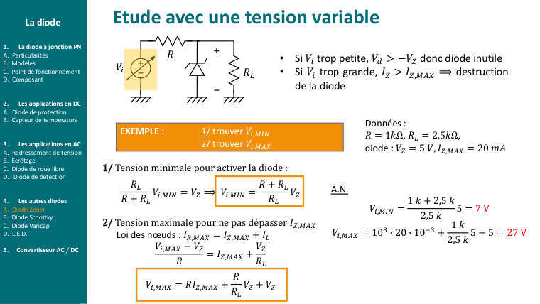
\(V_{i}=12\,\mathrm{V},\,\allowbreak R=220\,\mathrm{\Omega },\,\allowbreak V_{Z}=5{,}1\,\mathrm{V},\,\allowbreak I_{Z,\,\mathrm{max}}=50\,\mathrm{mA},\,\allowbreak I_{Z,\,\mathrm{min}}=1\,\mathrm{mA}\). Charge \(R_{L}\) variable.
Ce qu'on cherche(1) Vérifier que la Zener survit sans charge. \((2)\,R_{L,\,\mathrm{min}}\) pour rester régulé. (3) Puissance dans \(R\) et dans la Zener.
Courant dans \(R\) (constant tant que la régulation tient)
\(\displaystyle I_{R}=\frac{V_{i}-V_{Z}}{R}=\frac{12-5{,}1}{220}=\frac{6{,}9}{220}\approx 31{,}4\,\mathrm{mA}\)
Sans charge : tout passe dans la Zener
\(I_{Z}=I_{R}=31{,}4\,\mathrm{mA}\lt I_{Z,\,\mathrm{max}}=50\,\mathrm{mA}\) ✓. Puissance dissipée : \(P_{Z}=5{,}1\,\cdot \,0{,}0314\approx 0{,}16\,\mathrm{W}\) (choisir une Zener \(0{,}5\,\mathrm{W}\)).
Avec charge : loi des nœuds
\(\displaystyle I_{R}=I_{Z}+I_{L}\Longrightarrow I_{L}=I_{R}-I_{Z}\)
\(\displaystyle \text{Régulation maintenue tant que }\,I_{Z}\ge I_{Z,\,\mathrm{min}}\Longrightarrow I_{L}\le I_{R}-I_{Z,\,\mathrm{min}}=31{,}4-1=30{,}4\,\mathrm{mA}\)
\(\displaystyle R_{L,\,\mathrm{min}}=V_{Z}\,/\,I_{L,\,\mathrm{max}}=5{,}1\,/\,0{,}0304\approx 168\,\mathrm{\Omega }\)
Formule du cours \((I_{Z,\,\mathrm{min}}=0)\)
\(\displaystyle R_{L,\,\mathrm{min}}=V_{Z}\,\cdot \,R\,/\,(V_{i}-V_{Z})=5{,}1\,\cdot \,220\,/\,6{,}9\approx 163\,\mathrm{\Omega }\)
Même résultat à 3 % près ; la version avec \(I_{Z,\,\mathrm{min}}\) est plus sûre.
Si \(R_{L}\lt R_{L,\,\mathrm{min}}\) ?
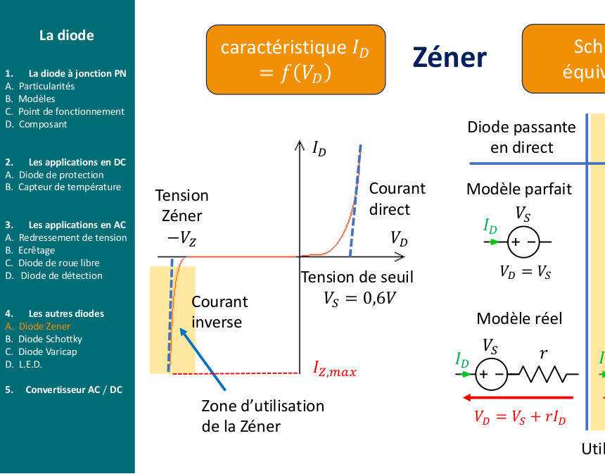
La Zener se bloque \((I_{Z}=0)\), le circuit redevient un simple diviseur \(\frac{R}{R_{L}}\colon V_{\mathrm{out}}=12\cdot \frac{R_{L}}{220+R_{L}}\lt 5{,}1\,\mathrm{V}\). Plus de régulation.
Réponse\(I_{R}\approx 31\,\mathrm{mA}\) ; sans charge OK \((P_{Z}\approx 0{,}16\,\mathrm{W});\,\allowbreak R_{L,\,\mathrm{min}}\approx 165-170\,\mathrm{\Omega }\).
Le raisonnement en « budget de courant »\(R\) fournit un courant fixe \(I_{R}\). La charge en prend ce qu'elle veut, la Zener absorbe le reste. Quand le reste devient nul, la régulation lâche. Le problème inverse (\(V_{i}\) variable, \(R_{L}\) fixe) se traite pareil : \(V_{i,\,\mathrm{min}}\) tel que \(I_{R}\ge I_{L}+I_{Z,\,\mathrm{min}},\,\allowbreak V_{i,\,\mathrm{max}}\) tel que \(I_{R}\le I_{L}+I_{Z,\,\mathrm{max}}\).
E8Ch. 4 · Polarisation par la base
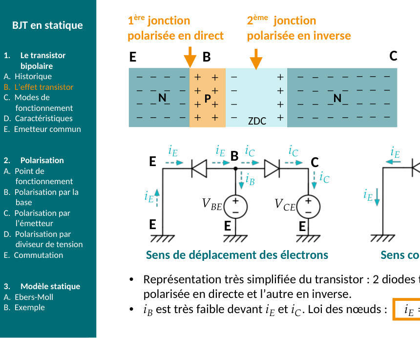
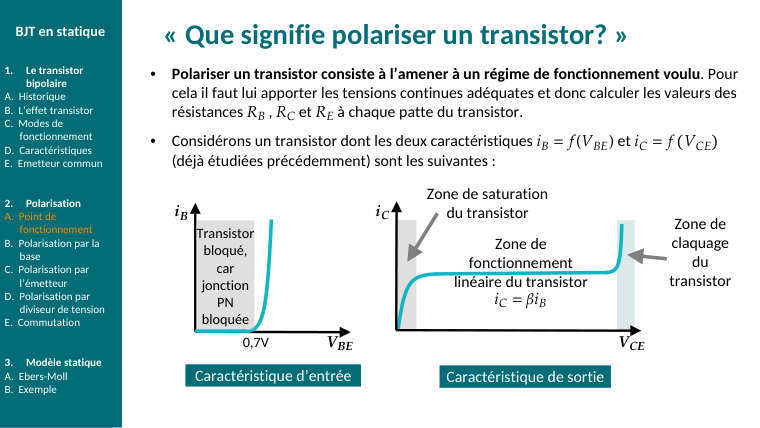
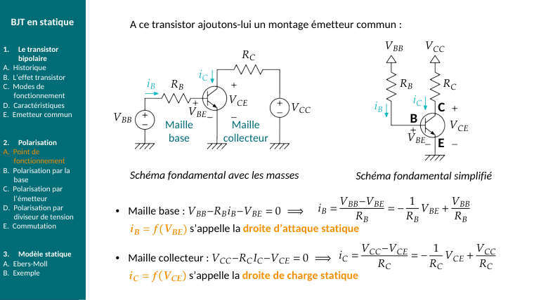
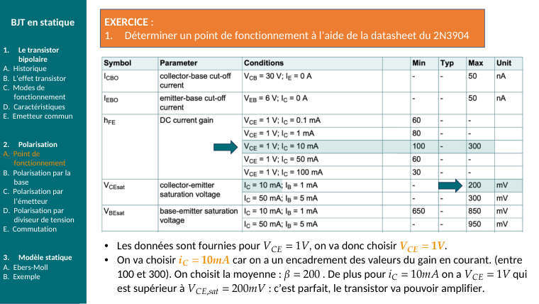
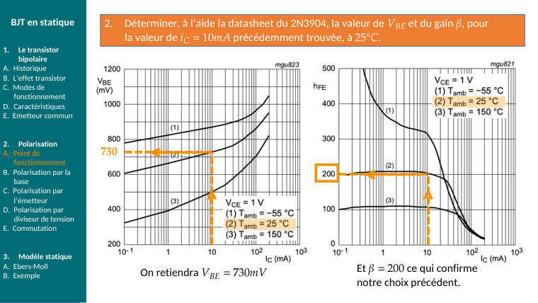
\(V_{\mathrm{CC}}=12\,\mathrm{V},\,\allowbreak V_{\mathrm{BB}}=5\,\mathrm{V},\,\allowbreak R_{B}=100\,\mathrm{k\Omega },\,\allowbreak R_{C}=1\,\mathrm{k\Omega }\). Point \(Q\) pour \(\beta =100\), puis \(\beta =300\).
Ce qu'on cherche\((I_{B},\,\allowbreak I_{C},\,\allowbreak V_{\mathrm{CE}})\) et le mode. Puis montrer pourquoi cette polarisation est « \(\beta\)-dépendante ».
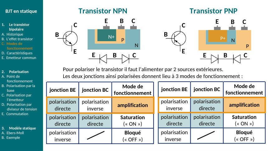
Hypothèse : mode actif, \(V_{\mathrm{BE}}=0{,}7\,\mathrm{V}\). Maille de base
\(\displaystyle I_{B}=\frac{V_{\mathrm{BB}}-V_{\mathrm{BE}}}{R_{B}}=\frac{5-0{,}7}{100}\,\mathrm{k}=43\,\mu A\)
Courant de collecteur et maille de collecteur \((\beta =100)\)
\(\displaystyle I_{C}=\beta \,I_{B}=4{,}3\,\mathrm{mA}\)
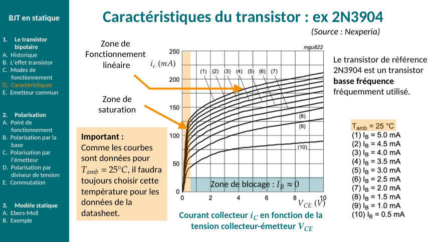
\(\displaystyle V_{\mathrm{CE}}=V_{\mathrm{CC}}-R_{C}\,I_{C}=12-1\,\mathrm{k}\,\cdot \,4{,}3\,\mathrm{m}=7{,}7\,\mathrm{V}\gt 0{,}2\,\mathrm{V}\text{ ✓ mode actif confirmé}\)
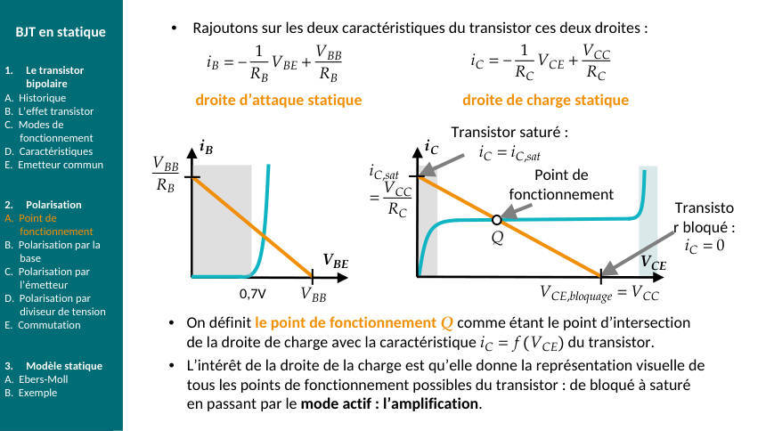
Droite de charge et saturation
\(\displaystyle I_{C,\,\mathrm{sat}}=V_{\mathrm{CC}}\,/\,R_{C}=12\,\mathrm{mA}\,(\text{à }\,V_{\mathrm{CE}}\approx 0)\)
\(Q=(7{,}7\,\mathrm{V};\,\allowbreak 4{,}3\,\mathrm{mA})\) est à peu près au milieu de la droite de charge : bon pour amplifier.
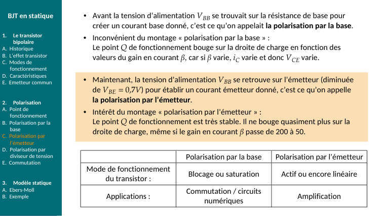
Même circuit, \(\beta =300\) (autre exemplaire, ou \(T\) plus élevée)
\(\displaystyle I_{C}=300\,\cdot \,43\,\mu =12{,}9\,\mathrm{mA}\gt I_{C,\,\mathrm{sat}}=12\,\mathrm{mA}\Longrightarrow \text{ IMPOSSIBLE }\Longrightarrow \text{ transistor SATURÉ}\)
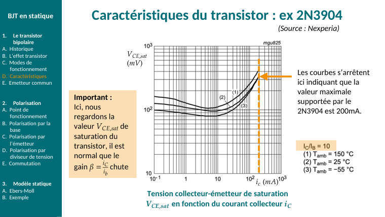
\(\displaystyle \text{On plafonne }\colon I_{C}=I_{C,\,\mathrm{sat}}\approx 12\,\mathrm{mA},\,\allowbreak V_{\mathrm{CE}}=V_{\mathrm{CE},\,\mathrm{sat}}\approx 0{,}1-0{,}2\,\mathrm{V}\)
Réponse\(\beta =100\) : actif, \(Q=(7{,}7\,\mathrm{V};\,\allowbreak 4{,}3\,\mathrm{mA})\). \(\beta =300\) : saturé, \(V_{\mathrm{CE}}\approx 0{,}2\,\mathrm{V}\). Le point \(Q\) dépend de \(\beta \Longrightarrow\) mauvaise polarisation pour un ampli, très bien pour un interrupteur.
Le test de saturation, toujoursAprès \(I_{C}=\beta I_{B}\), comparer à \(I_{C,\,\mathrm{sat}}\). Un \(V_{\mathrm{CE}}\) négatif dans la maille de collecteur est le signal d'alarme : ça veut dire « saturé ». En commutation on veut \(\beta \cdot I_{B}\gg I_{C,\,\mathrm{sat}}\) (facteur 2 à 10 de sécurité).
E9Ch. 4 · Polarisation par pont diviseur
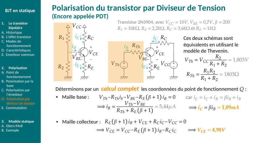
\(V_{\mathrm{CC}}=12\,\mathrm{V},\,\allowbreak R_{1}=10\,\mathrm{k\Omega },\,\allowbreak R_{2}=2{,}2\,\mathrm{k\Omega },\,\allowbreak R_{E}=2{,}2\,\mathrm{k\Omega },\,\allowbreak R_{C}=3{,}3\,\mathrm{k\Omega },\,\allowbreak \beta =150\)
Ce qu'on chercheLe point \(Q\) par la méthode Thévenin-sur-la-base, la vérification de la condition de « vraie source », et pourquoi \(Q\) ne dépend presque plus de \(\beta\).
Thévenin vu de la base
\(\displaystyle V_{\mathrm{Th}}=V_{\mathrm{CC}}\,\cdot \,\frac{R_{2}}{R_{1}+R_{2}}=12\,\cdot \,\frac{2{,}2}{12{,}2}\approx 2{,}16\,\mathrm{V}\)
\(\displaystyle R_{\mathrm{Th}}=R_{1}//R_{2}=10\cdot \frac{2{,}2}{12{,}2}\approx 1{,}80\,\mathrm{k\Omega }\)
Condition de stabilité
\(\displaystyle R_{\mathrm{Th}}\lt 0{,}01\cdot (\beta +1)\cdot R_{E}=0{,}01\,\cdot \,151\,\cdot \,2{,}2\,\mathrm{k}=3{,}32\,\mathrm{k\Omega }\Longrightarrow 1{,}80\,\mathrm{k}\lt 3{,}32\,\mathrm{k}\text{ ✓}\)
Le pont se comporte comme une vraie source de tension : le courant de base ne le « charge » pas.
Méthode rapide (\(\beta\)-indépendante)
\(\displaystyle V_{E}=V_{\mathrm{Th}}-V_{\mathrm{BE}}=2{,}16-0{,}7=1{,}46\,\mathrm{V}\)
\(\displaystyle I_{E}=V_{E}\,/\,R_{E}=1{,}46\,/\,2{,}2\,\mathrm{k}\approx 0{,}66\,\mathrm{mA}\approx I_{C}\)
\(\displaystyle V_{C}=V_{\mathrm{CC}}-R_{C}\,I_{C}=12-3{,}3\,\mathrm{k}\,\cdot \,0{,}66\,\mathrm{m}\approx 9{,}8\,\mathrm{V}\)
\(\displaystyle V_{\mathrm{CE}}=V_{C}-V_{E}\approx 9{,}8-1{,}46\approx 8{,}4\,\mathrm{V}\gt 0{,}2\text{ ✓ actif}\)
Méthode exacte (pour voir l'écart)
\(\displaystyle \text{Maille base }\colon V_{\mathrm{Th}}-R_{\mathrm{Th}}\,I_{B}-V_{\mathrm{BE}}-R_{E}\,(\beta +1)\,I_{B}=0\)
\(\displaystyle I_{B}=1{,}46\,/\,(1{,}8\,\mathrm{k}+151\,\cdot \,2{,}2\,\mathrm{k})=1{,}46\,/\,334\,\mathrm{k}\approx 4{,}4\,\mu A\Longrightarrow I_{C}=150\,\cdot \,4{,}4\,\mu \approx 0{,}66\,\mathrm{mA}\)
Identique à 1 % près. Avec \(\beta =300\colon I_{B}=\frac{1{,}46}{(1{,}8\,\mathrm{k}+662\,\mathrm{k})}=2{,}2\,\mu A,\,\allowbreak I_{C}=0{,}66\,\mathrm{mA}\) —
inchangé. C'est tout l'intérêt de \(R_{E}\).
Réponse\(Q\approx (V_{\mathrm{CE}}=8{,}4\,\mathrm{V};\,\allowbreak I_{C}=0{,}66\,\mathrm{mA})\), stable en \(\beta\).
Pourquoi \(R_{E}\) stabiliseSi \(\beta\) augmente, \(I_{C}\) veut augmenter \(\Longrightarrow V_{E}=R_{E}I_{E}\) augmente \(\Longrightarrow V_{\mathrm{BE}}=V_{B}-V_{E}\) diminue \(\Longrightarrow I_{B}\) diminue \(\Longrightarrow I_{C}\) revient. C'est une contre-réaction, comme dans l'AOP.
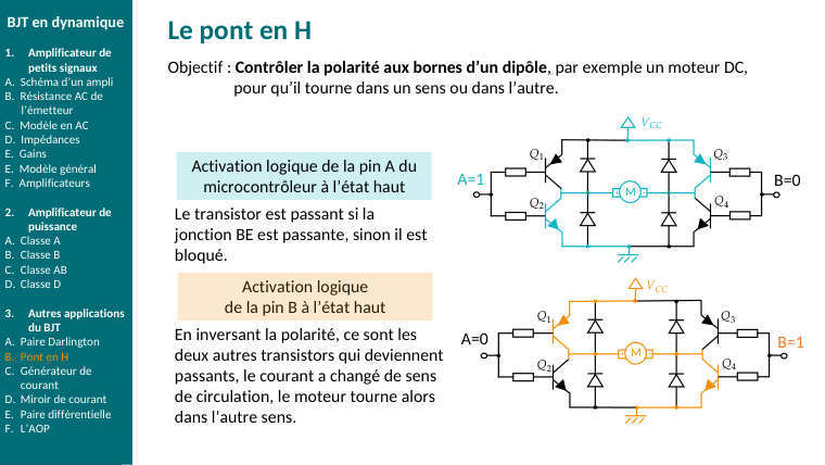
E10Ch. 5 · Émetteur commun en AC
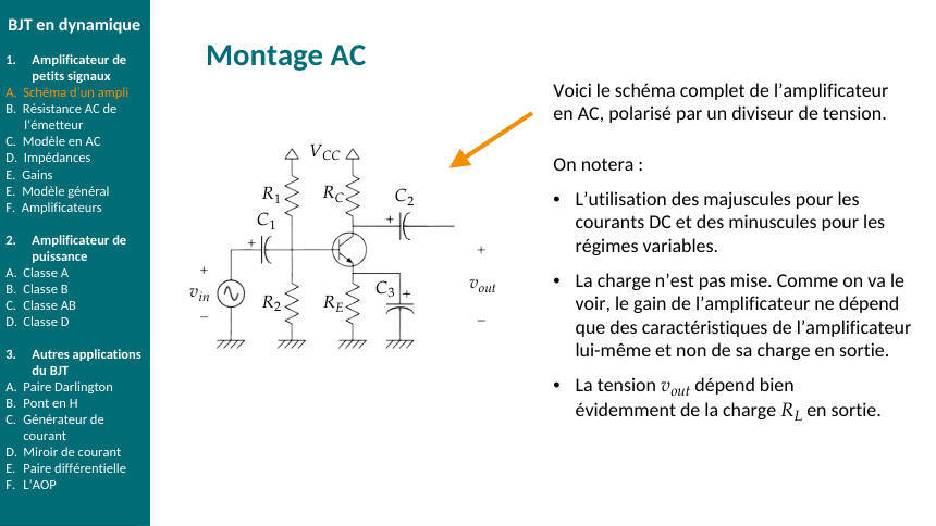
Même montage que E9 \((I_{E}=0{,}66\,\mathrm{mA})\), avec \(C_{1},\,\allowbreak C_{2}\) de liaison et \(C_{3}\) de découplage sur \(R_{E}\). Charge \(R_{L}=10\,\mathrm{k\Omega }\).
Ce qu'on cherche\(r_{E},\,\allowbreak A_{V}\) à vide et en \(\mathrm{d}B,\,\allowbreak Z_{\mathrm{in}},\,\allowbreak Z_{\mathrm{out}}\), gain avec la charge, et gain sans \(C_{3}\).
Résistance dynamique d'émetteur (à partir du DC)
\(\displaystyle r_{E}=26\,\mathrm{mV}\,/\,I_{E}=26\,/\,0{,}66\approx 39\,\mathrm{\Omega }\)
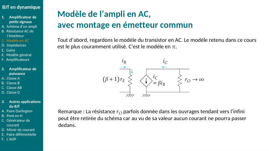
Schéma AC : \(C\) = fils, \(V_{\mathrm{CC}}\) = masse, \(R_{E}\) court-circuitée par \(C_{3}\)
Entrée : \(R_{1}\) et \(R_{2}\) tous deux entre base et masse (\(V_{\mathrm{CC}}\) est à la masse en AC) ⟹ en parallèle avec \((\beta +1)r_{E}\). Sortie : \(R_{C}\) entre collecteur et masse.
Gains et impédances
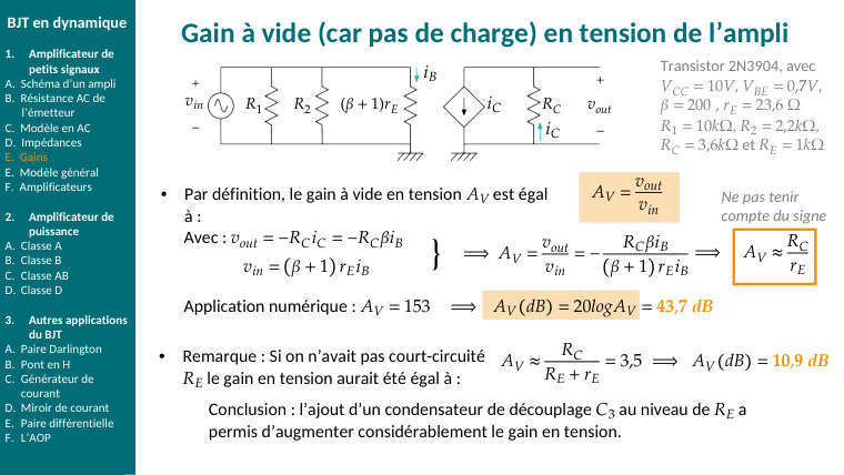
\(\displaystyle A_{V}=-R_{C}\,/\,r_{E}=-3300\,/\,39\approx -84\Longrightarrow 20\cdot \log (84)\approx 38{,}5\,\mathrm{d}B,\,\allowbreak \text{ déphasage }\,180\text{°}\)
\(\displaystyle Z_{\mathrm{in}}=R_{1}//R_{2}//(\beta +1)\,r_{E}=1{,}8\,\mathrm{k}//(151\,\cdot \,39=5{,}9\,\mathrm{k})\approx 1{,}38\,\mathrm{k\Omega }\)
\(\displaystyle Z_{\mathrm{out}}=R_{C}=3{,}3\,\mathrm{k\Omega }\)
Avec la charge \(R_{L}\) (diviseur de tension en sortie)
\(\displaystyle A_{V,\,\mathrm{charg}}\text{é }=A_{V}\,\cdot \,\frac{R_{L}}{Z_{\mathrm{out}}+R_{L}}=-84\,\cdot \,\frac{10}{13{,}3}\approx -63\,\left(\text{équivalent }\colon -\frac{R_{C}//R_{L}}{r_{E}}=-2{,}48\,\mathrm{k}/39\approx -63\right)\)
Sans \(C_{3}\)
\(\displaystyle A_{V}=-R_{C}\,/\,(R_{E}+r_{E})=-3300\,/\,2239\approx -1{,}5\)
Le découplage multiplie le gain par ~57. En échange, sans \(C_{3}\) le gain \(\approx \frac{-R_{C}}{R_{E}}\) est
indépendant de \(r_{E}\), donc de la température : compromis gain / stabilité.
Réponse\(r_{E}\approx 39\,\mathrm{\Omega };\,\allowbreak A_{V}\approx -84\,(38{,}5\,\mathrm{d}B);\,\allowbreak Z_{\mathrm{in}}\approx 1{,}4\,\mathrm{k\Omega };\,\allowbreak Z_{\mathrm{out}}=3{,}3\,\mathrm{k\Omega }\) ; chargé \(\approx -63\) ; sans \(C_{3}\approx -1{,}5\).
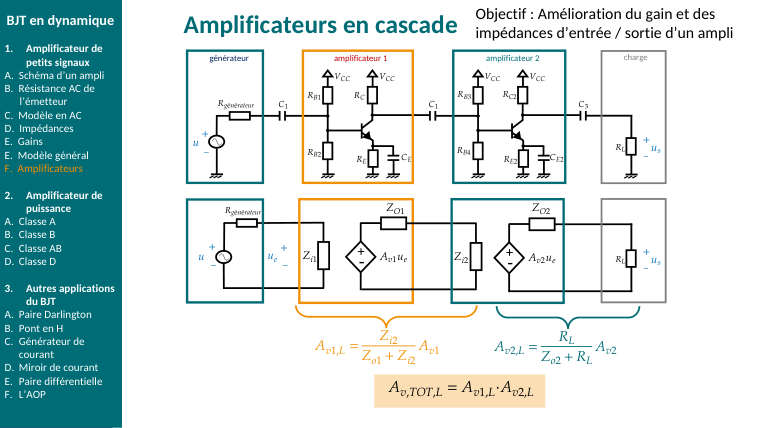
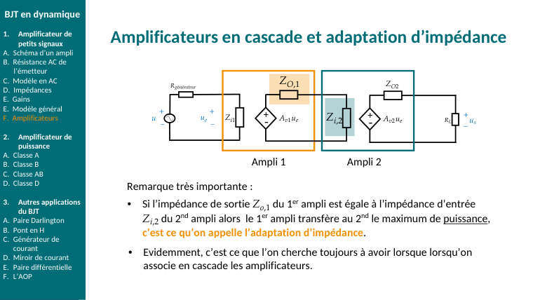
Le fil conducteurTout le chapitre 5 tient dans : \(Q\) (DC) \(\Longrightarrow r_{E}\Longrightarrow\) modèle en \(\pi \Longrightarrow\) trois nombres \((A_{V},\,\allowbreak Z_{\mathrm{in}},\,\allowbreak Z_{\mathrm{out}})\). Ensuite l'ampli est une boîte noire qu'on charge ou qu'on cascade avec des diviseurs de tension.
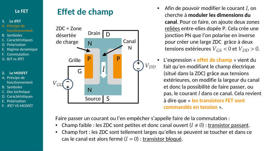
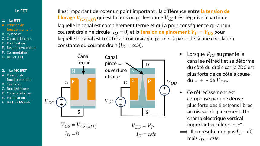
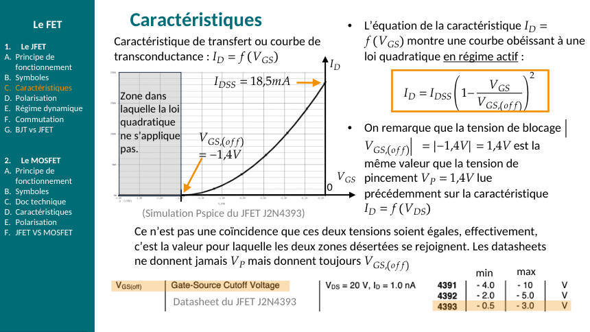
E11Ch. 6 · JFET autopolarisé
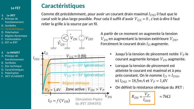
\(I_{\mathrm{DSS}}=10\,\mathrm{mA},\,\allowbreak V_{\mathrm{GS},\,\mathrm{off}}=-4\,\mathrm{V},\,\allowbreak R_{S}=500\,\mathrm{\Omega },\,\allowbreak R_{D}=1\,\mathrm{k\Omega },\,\allowbreak V_{\mathrm{DD}}=15\,\mathrm{V}\), grille à la masse par \(R_{G}\)
Ce qu'on chercheLe point de repos \((V_{\mathrm{GS}},\,\allowbreak I_{D},\,\allowbreak V_{\mathrm{DS}})\), la vérification de la zone active, puis \(g_{m}\) et le gain en source commune.
Équation de la maille grille-source
\(I_{G}=0\Longrightarrow V_{G}=0;\,\allowbreak V_{S}=R_{S}\,I_{D}\Longrightarrow\)
\(\displaystyle V_{\mathrm{GS}}=-R_{S}\,\cdot \,I_{D}=-0{,}5\,\cdot \,I_{D}\,(V\text{ en volts},\,\allowbreak I_{D}\text{ en }\,mA)\)
Injecter dans la loi quadratique
\(\displaystyle I_{D}=I_{\mathrm{DSS}}\,\left(1-\frac{V_{\mathrm{GS}}}{V_{\mathrm{GS},\,\mathrm{off}}}\right)^{2}=10\,\left(1-\frac{(-0{,}5\,I_{D})}{-4}\right)^{2}=10\,(1-0{,}125\,I_{D})^{2}\)
\(\displaystyle I_{D}=10-2{,}5\,I_{D}+0{,}15625\,I_{D}^{2}\Longrightarrow 0{,}15625\,I_{D}^{2}-3{,}5\,I_{D}+10=0\)
Résoudre et choisir la racine
\(\displaystyle \Delta =3{,}5^{2}-4\,\cdot \,0{,}15625\,\cdot \,10=12{,}25-6{,}25=6\Longrightarrow \sqrt{\Delta }\approx 2{,}45\)
\(\displaystyle I_{D}=\frac{(3{,}5\,\pm \,2{,}45)}{(2\,\cdot \,0{,}15625)}=\frac{(3{,}5\,\pm \,2{,}45)}{0{,}3125}\Longrightarrow 19{,}0\,\mathrm{mA}\text{ ou }\,3{,}36\,\mathrm{mA}\)
\(19\,\mathrm{mA}\gt I_{\mathrm{DSS}}\) et donnerait \(V_{\mathrm{GS}}=-9{,}5\,\mathrm{V}\lt V_{\mathrm{GS},\,\mathrm{off}}\) : impossible. On garde
\(I_{D}=3{,}36\,\mathrm{mA}\), \(V_{\mathrm{GS}}=-1{,}68\,\mathrm{V}\) (bien entre −4 et 0 ✓).
\(V_{\mathrm{DS}}\) et zone de fonctionnement
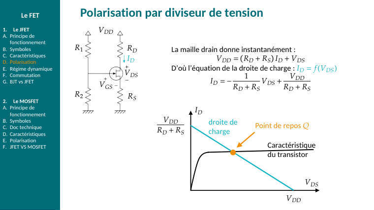
\(\displaystyle V_{\mathrm{DS}}=V_{\mathrm{DD}}-(R_{D}+R_{S})\,I_{D}=15-1{,}5\,\mathrm{k}\,\cdot \,3{,}36\,\mathrm{m}\approx 10\,\mathrm{V}\)
\(\displaystyle \text{Condition zone active }\colon V_{\mathrm{DS}}\gt V_{\mathrm{GS}}-V_{\mathrm{GS},\,\mathrm{off}}=-1{,}68+4=2{,}3\,\mathrm{V}\Longrightarrow 10\gt 2{,}3\text{ ✓}\)
Transconductance et gain (source commune, \(R_{S}\) découplée)
\(\displaystyle g_{m}=(2\,I_{\mathrm{DSS}}/|V_{P}|)\left(1-\frac{V_{\mathrm{GS}}}{V_{\mathrm{GS},\,\mathrm{off}}}\right)=(20\,\mathrm{m}/4)(1-0{,}42)=5\,\mathrm{m}\,\cdot \,0{,}58\approx 2{,}9\,\mathrm{mS}\)
\(\displaystyle A_{V}=-g_{m}\,R_{D}=-2{,}9\,\mathrm{m}\,\cdot \,1\,\mathrm{k}\approx -2{,}9\)
Faible gain : c'est la contrepartie de l'impédance d'entrée énorme du FET.
Réponse\(I_{D}\approx 3{,}4\,\mathrm{mA},\,\allowbreak V_{\mathrm{GS}}\approx -1{,}7\,\mathrm{V},\,\allowbreak V_{\mathrm{DS}}\approx 10\,\mathrm{V}\) (zone active) ; \(g_{m}\approx 2{,}9\,\mathrm{mS},\,\allowbreak A_{V}\approx -2{,}9\).
Sans calcul : la méthode graphiqueTracer la parabole \(I_{D}(V_{\mathrm{GS}})\) entre \(V_{\mathrm{GS},\,\mathrm{off}}\) et 0, et la droite \(V_{\mathrm{GS}}=-R_{S}I_{D}\) (passe par l'origine, pente \(\frac{-1}{R_{S}}\)). L'intersection est \(Q\). Utile pour vérifier l'ordre de grandeur de la racine choisie.
E12Ch. 6 · MOSFET
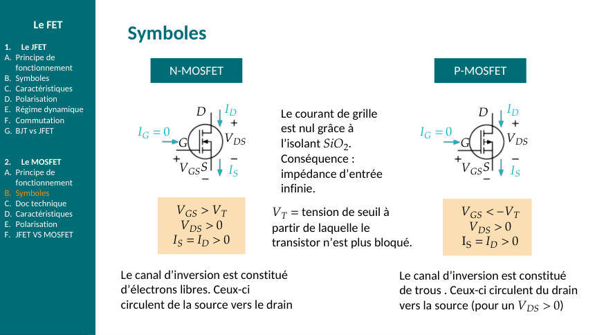
\(N\)-MOS avec \(K_{n}\cdot \frac{W}{L}=2\,\mathrm{mA}/\,\mathrm{V}^{2},\,\allowbreak V_{T}=1\,\mathrm{V},\,\allowbreak V_{\mathrm{GS}}=3\,\mathrm{V},\,\allowbreak V_{\mathrm{DD}}=10\,\mathrm{V}\). \((a)\,R_{D}=1{,}5\,\mathrm{k\Omega };\,\allowbreak (b)\,R_{D}=5\,\mathrm{k\Omega }\).
Ce qu'on chercheLa région de fonctionnement et \(I_{D},\,\allowbreak V_{\mathrm{DS}},\,\allowbreak g_{m}\). Méthode : supposer saturé, vérifier \(V_{\mathrm{DS}}\ge V_{\mathrm{GS}}-V_{T}\).
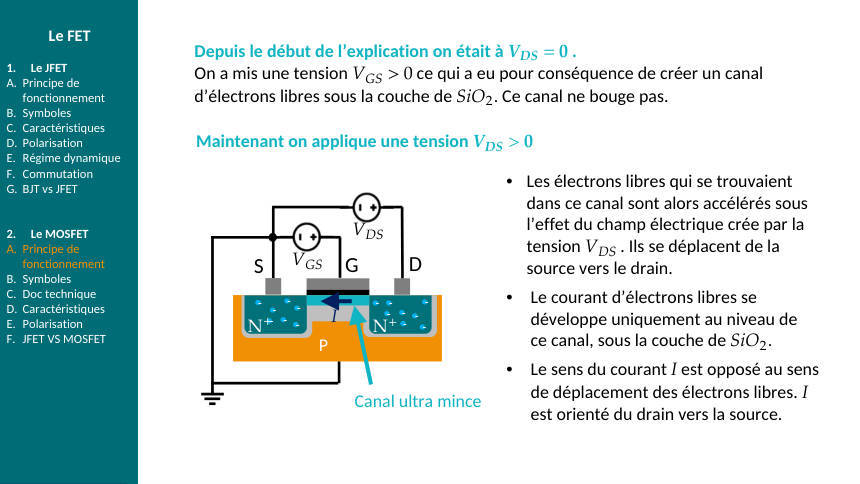
Le transistor conduit-il ?
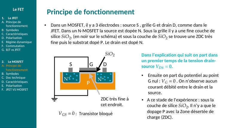
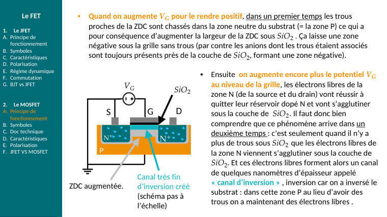
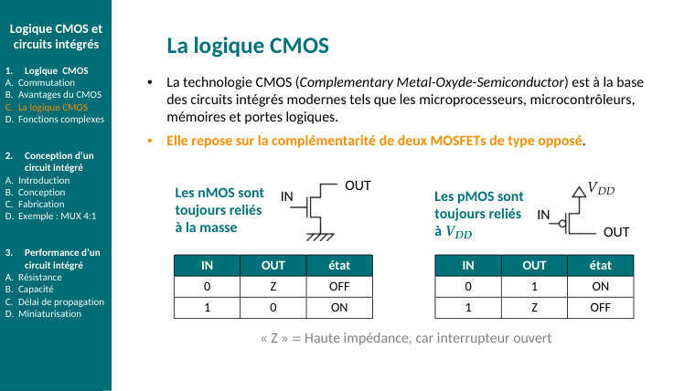
\(V_{\mathrm{GS}}=3\,\mathrm{V}\gt V_{T}=1\,\mathrm{V}\Longrightarrow\) canal d'inversion formé ⟹ conduit. Tension de commande utile : \(V_{\mathrm{GS}}-V_{T}=2\,\mathrm{V}\).
Hypothèse « saturé » (zone active)
\(\displaystyle I_{D}=\frac{1}{2}\,\cdot \,K_{n}\,\left(\frac{W}{L}\right)\,\cdot \,(V_{\mathrm{GS}}-V_{T})^{2}=\frac{1}{2}\,\cdot \,2\,\mathrm{m}\,\cdot \,2^{2}=4\,\mathrm{mA}\)
\((a)\,R_{D}=1{,}5\,\mathrm{k\Omega }\) — vérification
\(\displaystyle V_{\mathrm{DS}}=V_{\mathrm{DD}}-R_{D}\,I_{D}=10-1{,}5\,\mathrm{k}\,\cdot \,4\,\mathrm{m}=4\,\mathrm{V}\ge V_{\mathrm{GS}}-V_{T}=2\,\mathrm{V}\text{ ✓ saturé confirmé}\)
\(\displaystyle g_{m}=2\,\frac{I_{D}}{V_{\mathrm{GS}}-V_{T}}=8\,\mathrm{m}\,/\,2=4\,\mathrm{mS}\)
\((b)\,R_{D}=5\,\mathrm{k\Omega }\) — vérification
\(\displaystyle V_{\mathrm{DS}}=10-5\,\mathrm{k}\,\cdot \,4\,\mathrm{m}=-10\,\mathrm{V}\Longrightarrow \text{ absurde }\,(V_{\mathrm{DS}}\lt 0)\)
L'hypothèse est fausse : le transistor est en
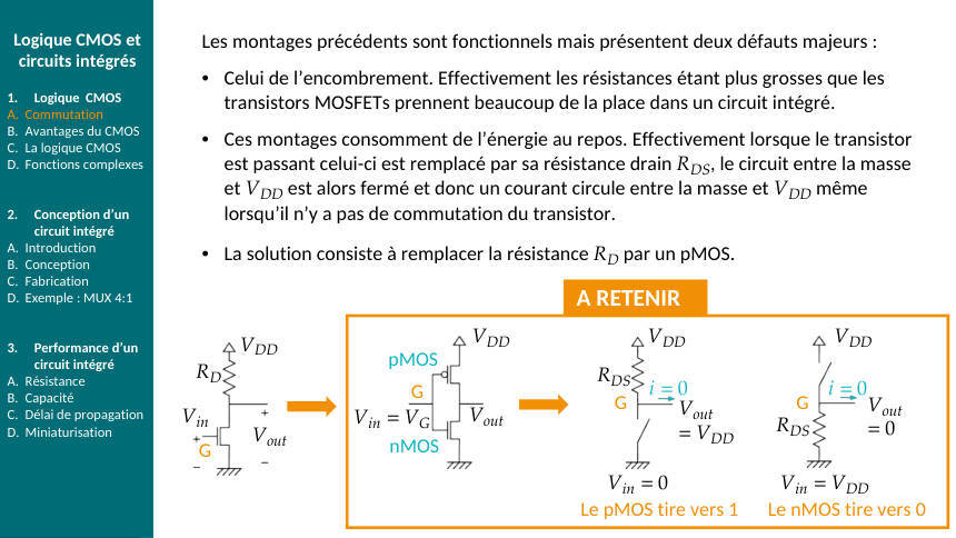
région ohmique (canal non pincé). \(I_{D}\) est plus petit que \(4\,\mathrm{mA}\) et \(V_{\mathrm{DS}}\) est petit ; il se comporte comme une résistance \(R_{\mathrm{DS}}\approx \frac{1}{K_{n}\left(\frac{W}{L}\right)(V_{\mathrm{GS}}-V_{T})}=250\,\mathrm{\Omega }\), d'où \(V_{\mathrm{DS}}\approx 10\,\cdot \,\frac{250}{5250}\approx 0{,}5\,\mathrm{V}\). C'est le régime « interrupteur fermé » du chapitre 7.
Réponse(a) saturé : \(I_{D}=4\,\mathrm{mA},\,\allowbreak V_{\mathrm{DS}}=4\,\mathrm{V},\,\allowbreak g_{m}=4\,\mathrm{mS}\). \((b)\) ohmique : \(V_{\mathrm{DS}}\approx 0{,}5\,\mathrm{V}\), le MOS agit en interrupteur fermé.
Trois régions, un seul test\(V_{\mathrm{GS}}\lt V_{T}\) : bloqué. Sinon, \(V_{\mathrm{DS}}\ge V_{\mathrm{GS}}-V_{T}\) : saturé (source de courant, pour amplifier). \(V_{\mathrm{DS}}\lt V_{\mathrm{GS}}-V_{T}\) : ohmique (résistance commandée, pour commuter). Le MOSFET logique (ch. 7) vit dans bloqué/ohmique, jamais en saturé.
E13Ch. 7 · Synthèse CMOS
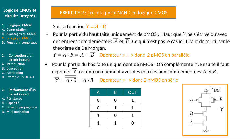
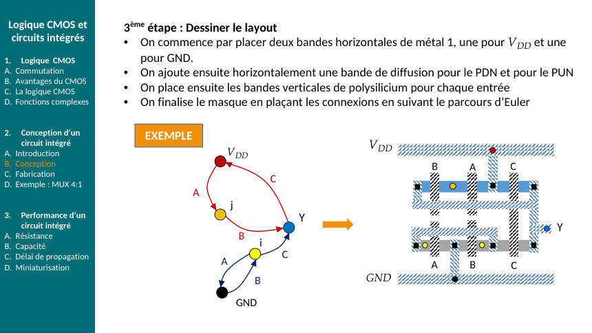
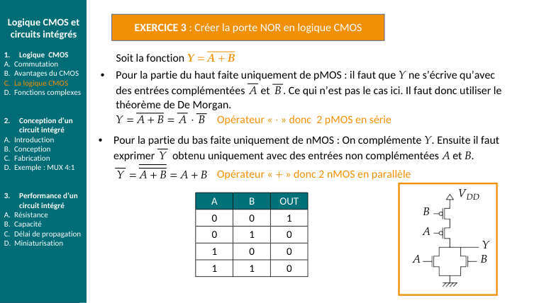
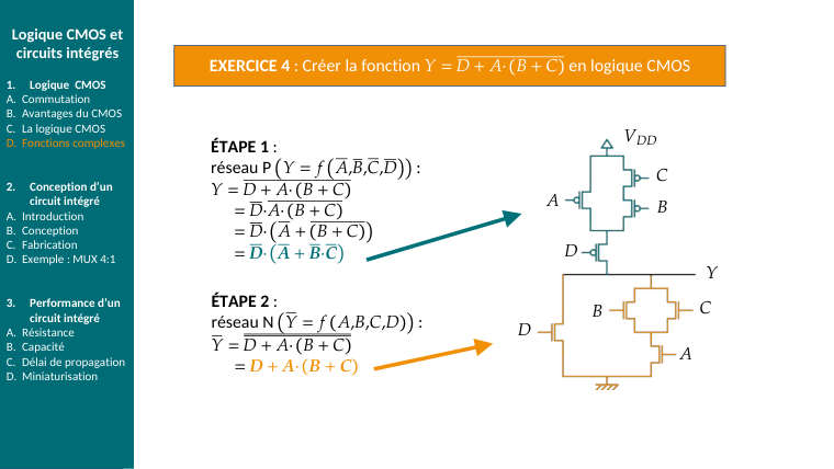
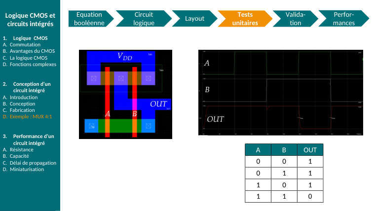
Réaliser \(Y\) = \(A\cdot B+C\) en logique CMOS et compter les transistors
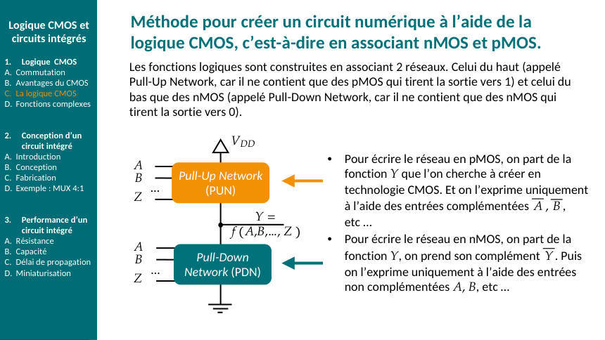
Ce qu'on chercheLe réseau PDN (nMOS, vers GND) et le réseau PUN (pMOS, vers \(V_{\mathrm{DD}}\)), puis la vérification sur la table de vérité.
PDN : partir de \(\bar{Y}\), entrées non complémentées
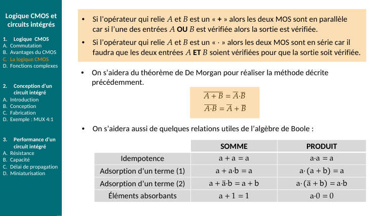
\(\displaystyle \bar{Y}=A\cdot B+C\Longrightarrow \text{ « }\,\cdot \text{ » }=\text{ série},\,\allowbreak \text{ « }+\text{ » }=\text{ parallèle}\)
\(\displaystyle PDN=(\text{nMOS}_{A}\text{ en série avec nMOS}_{B})\text{ en parallèle avec nMOS}_{C}\)
Lecture : la sortie est tirée à 0 si (\(A\) et \(B\)) ou si \(C\).
PUN : la structure duale (série ↔ parallèle), mêmes entrées, transistors pMOS
\(\displaystyle Y=\overline{(A\cdot B+C)}=\overline{(A\cdot B)}\,\cdot \,\bar{C}=(\bar{A}+\bar{B})\,\cdot \,\bar{C}\,(\text{De Morgan deux fois})\)
\(\displaystyle PUN=(\text{pMOS}_{A}\text{ en parallèle avec pMOS}_{B})\text{ en série avec pMOS}_{C}\)
Un pMOS conduit quand son entrée vaut 0 : la sortie est tirée à 1 si (\(A=0\) ou \(B=0\)) et \(C=0\). ✓ cohérent avec \(Y\).
Compter
3 entrées \(\Longrightarrow 3\) nMOS + 3 pMOS = 6 transistors. Règle : une fonction à \(n\) entrées réalisée en une seule porte complexe (AOI) coûte \(2\,\mathrm{n}\) transistors.
Vérifier une ligne de la table
\(A=1,\,\allowbreak B=1,\,\allowbreak C=0\) : PDN : \(A\cdot B\) conduit ⟹ chemin vers GND \(\Longrightarrow Y=0\). PUN : pMOS_A et pMOS_B tous deux ouverts ⟹ pas de chemin vers \(V_{\mathrm{DD}}\) ✓ (jamais les deux réseaux fermés en même temps : pas de court-circuit).
RéponsePDN : (\(A\) série \(B\)) // \(C\) ; PUN : \((A//B)\) série \(C;\,\allowbreak 6\) transistors.
Si la fonction n'est pas « inversée »\(Y=A\cdot B+C\) (sans barre) n'est pas réalisable en une seule porte CMOS (une porte CMOS statique est toujours inverseuse). On réalise \(A\cdot B+C\) \((6\,\mathrm{T})\) puis un inverseur \((2\,\mathrm{T})=8\) transistors. Même logique pour AND = NAND + NOT.
E14Ch. 7 · Résistances, capacités, délai
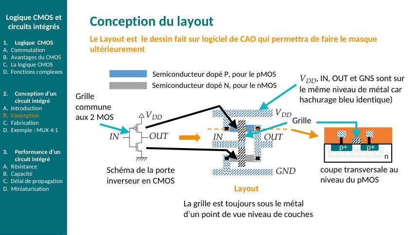
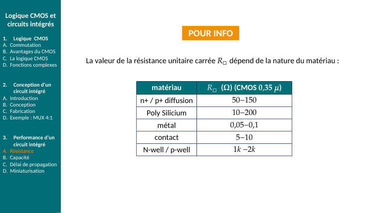
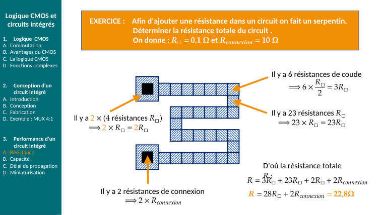
\(R_{\square }\)(métal) \(=0{,}1\,\mathrm{\Omega }\), rail de \(40\,\lambda \,\times \,4\,\lambda\) avec un coude ; \(R_{N}=R_{P}=5\,\mathrm{k\Omega };\,\allowbreak C_{\mathrm{OUT}}=20\,\mathrm{fF}\). Délai d'un inverseur, puis d'une NAND3.
Ce qu'on chercheAppliquer la méthode des carrés, puis le modèle RC du délai, puis la règle du carré du nombre de transistors en série.
Résistance du rail par comptage de carrés
\(\displaystyle \text{nombre de carrés }=\frac{\ell }{w}=\frac{40}{4}=10;\,\allowbreak \text{ un coude compte }\,\frac{1}{2}\text{ carré}\)
\(\displaystyle R_{\mathrm{rail}}=R_{\square }\,\cdot \,(10+0{,}5)=0{,}1\,\cdot \,10{,}5\approx 1{,}05\,\mathrm{\Omega }\)
Négligeable devant les \(5\,\mathrm{k\Omega }\) des transistors : c'est en général le cas pour le métal, pas pour le polysilicium (\(R_{\square }\) ~ \(10-50\,\mathrm{\Omega }\)).
Délai de l'inverseur
\(\displaystyle \tau =(R_{N}+R_{P})\,\cdot \,C_{\mathrm{OUT}}\,/\,2=(5\,\mathrm{k}+5\,\mathrm{k})\,\cdot \,20\,f\,/\,2=100\,\mathrm{ps}\)
NAND à 3 entrées : 3 nMOS en série dans le PDN
\(\displaystyle \tau _{\mathrm{descente}}\approx \left(\frac{n^{2}}{2}\right)\,\cdot \,R_{N}\,\cdot \,C=\left(\frac{9}{2}\right)\,\cdot \,5\,\mathrm{k}\,\cdot \,20\,f=450\,\mathrm{ps}\,(\text{Elmore})\)
\(\displaystyle \tau _{\mathrm{mont}}ée\colon \text{ les }\,3\text{ pMOS sont en parallèle }\Longrightarrow \text{ au pire un seul conduit }\colon R_{P}\,\cdot \,C=100\,\mathrm{ps}\)
Le délai « pire cas » est \(450\,\mathrm{ps}\) : la NAND3 est ~4,5 fois plus lente que l'inverseur sur le front descendant.
Fréquence \(\max\) et miniaturisation
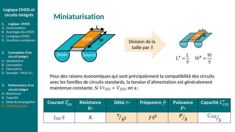
Chaîne de 5 portes de \(100\,\mathrm{ps}\) : chemin critique \(0{,}5\,\mathrm{ns}\Longrightarrow\) période \(\ge 1\,\mathrm{ns}\Longrightarrow f\lt 1\,\mathrm{GHz}\). En divisant les dimensions par \(S=2\) (\(V_{\mathrm{DD}}\) constant) : \(\tau \to \frac{\tau }{4},\,\allowbreak f\to 4f\).
Réponse\(R_{\mathrm{rail}}\approx 1\,\mathrm{\Omega };\,\allowbreak \tau _{\mathrm{inv}}=100\,\mathrm{ps};\,\allowbreak \tau _{\mathrm{NAND3}}\approx 450\,\mathrm{ps}\) (descente) / \(100\,\mathrm{ps}\) (montée).
Pourquoi \(n^{2}\) et pas \(n\)\(n\) transistors en série : la résistance totale est \(nR\) et chaque nœud intermédiaire porte sa capacité ; la somme des produits \(R\times C\) cumulés donne \(\approx \frac{n^{2}}{2}\). Conséquence de conception : on évite plus de 3–4 transistors en série et on met les entrées « tardives » près de la sortie.